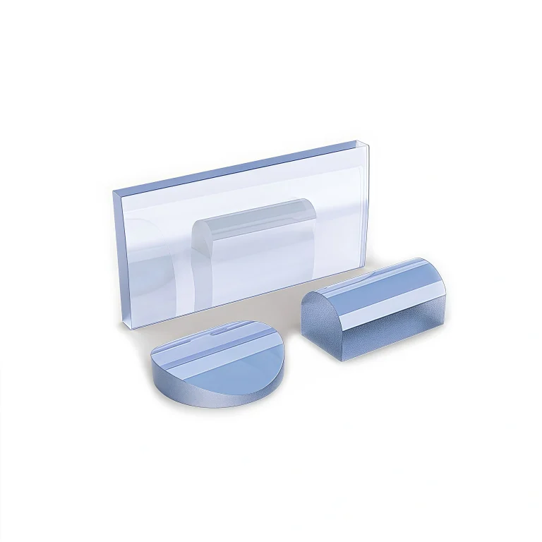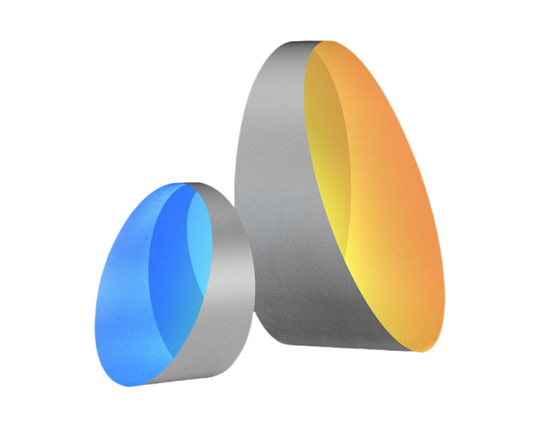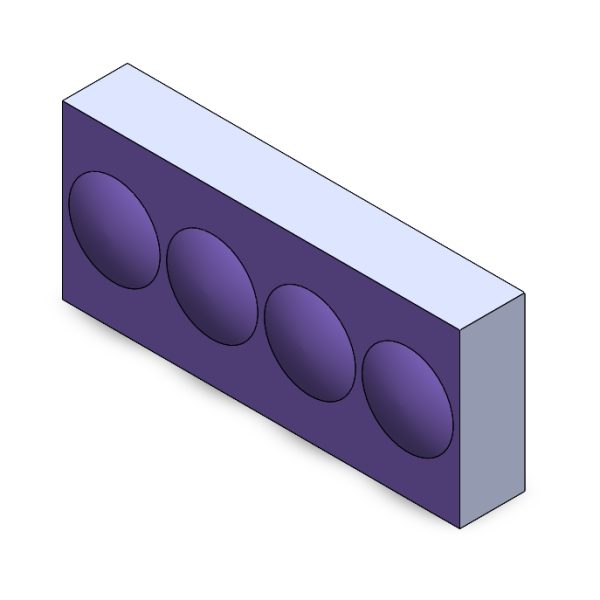
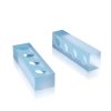
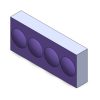
Lens arrays are structured with multiple identical or varying lenses arranged in formats such as linear arrays or two-dimensional matrices (square, hexagonal). Each sub-lens can perform individual functions like focusing, collimating, or diffusing light, enabling simultaneous multi-beam processing.
Structural Types:
- Linear Lens Arrays: One-dimensional cylindrical lens arrangement, ideal for line scanning and slit illumination.
- 2D Lens Arrays: Matrix layout for full-field light shaping, beam homogenization, and imaging applications.
- Aspherical Arrays: Correct optical aberrations and improve resolution in imaging systems.
- Tunable Lens Arrays: Electrically controlled focal length for adaptive optics and dynamic beam shaping.

Materials & Manufacturing:
- Materials: Optical glass (BK7, fused silica), polymers (PMMA, PC), silicon (for IR), flexible substrates (PDMS) for wearable and curved surfaces.
- Processes: Photolithographic reflow (for microlens arrays), injection molding (mass production), laser microfabrication (custom, high-precision).
Core Optical Features:
- Parallel Beam Processing: Each sub-lens modulates a distinct portion of the light field.
- Uniform Light Distribution: Transforms Gaussian beams into flat-top beams for consistent energy delivery.
- Field-of-View Expansion: Enhances wide-angle imaging and depth capture in systems like light field cameras.
- Miniaturization: Microlens arrays (MLAs) support on-chip integration in mobile devices and compact optical modules.
Application Fields:
- Imaging & Photography: Light field cameras, confocal microscopy, multi-view 3D displays.
- Laser Processing & Lithography: Beam shaping for laser engraving, wafer cutting, and uniform illumination in photolithography.
- Optical Communication & Sensing: Fiber coupling, VCSEL/PD arrays, LiDAR scanning, distributed fiber sensors.
- Consumer Electronics: Smartphone camera modules, VR/AR optics, optical fingerprint recognition.
- Scientific Research & Astronomy: Solar telescopes, quantum optics, and high-throughput optical experiments.