Expertise Note: The role of a TO package is not just to protect the chip – it is more like a fixed starting point. Once the package structure is finalized, the light emission position, angle, and alignment reference are essentially locked in. All subsequent optical design is then optimized based on this foundation.
Technical Review: This article is based on common packaging methods for optoelectronic devices (such as laser diodes and photodetectors). It analyzes the role of TO packages in optical systems from the perspectives of hermetic sealing, electrical lead-out methods, and optical interface characteristics, covering key factors such as insertion loss, reflection control, and alignment accuracy.
What Exactly is a TO Package?
A TO package (Transistor Outline package) is a standardized metal package structure commonly used in optoelectronic devices. It was originally used mainly for early transistors and optoelectronic devices, and later expanded to optical devices such as laser diodes and photodetectors, becoming a mature industrial packaging form.
The reason it exists is essentially to solve a practical problem: an optical chip cannot be used directly by itself. The chip needs stable mechanical support, reliable electrical connections, and must also provide a controllable optical output interface. Therefore, the TO package serves three core functions structurally: mechanical fixing, electrical lead-out, and optical window definition.
In terms of structural features, a TO package typically consists of a metal housing, pins, and a top optical window, using hermetic sealing to improve long-term stability. This structure not only protects the internal chip from environmental influences but also ensures consistency and reliability during long-term operation. As a result, it has been widely used in low-to-medium power optoelectronic devices for a long time.

Why is a TO Package Needed?
In practice, optical chips are rarely used directly exposed. This is due to considerations such as structural design and pollution prevention. The chip itself is very sensitive to its environment – dust, humidity, and even slight mechanical stress can affect its output stability. At the same time, optical systems have strict requirements for optical axis alignment, and the lack of a stable mechanical reference can significantly reduce coupling efficiency.
The TO package provides a stable mechanical mounting reference, standardized electrical connections, and a top optical window, converting an uncontrollable optical chip into a device suitable for engineering applications.
What is the Structure of a TO Package?
From a structural perspective, a TO package typically consists of a metal housing, an optical window, and pins – the result of balancing thermal, optical, and electrical requirements.
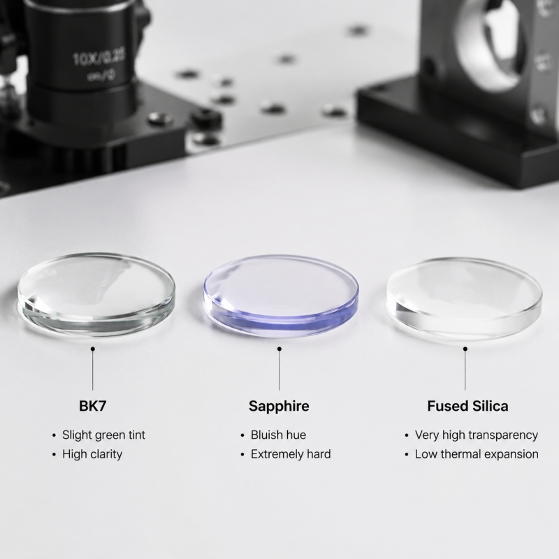
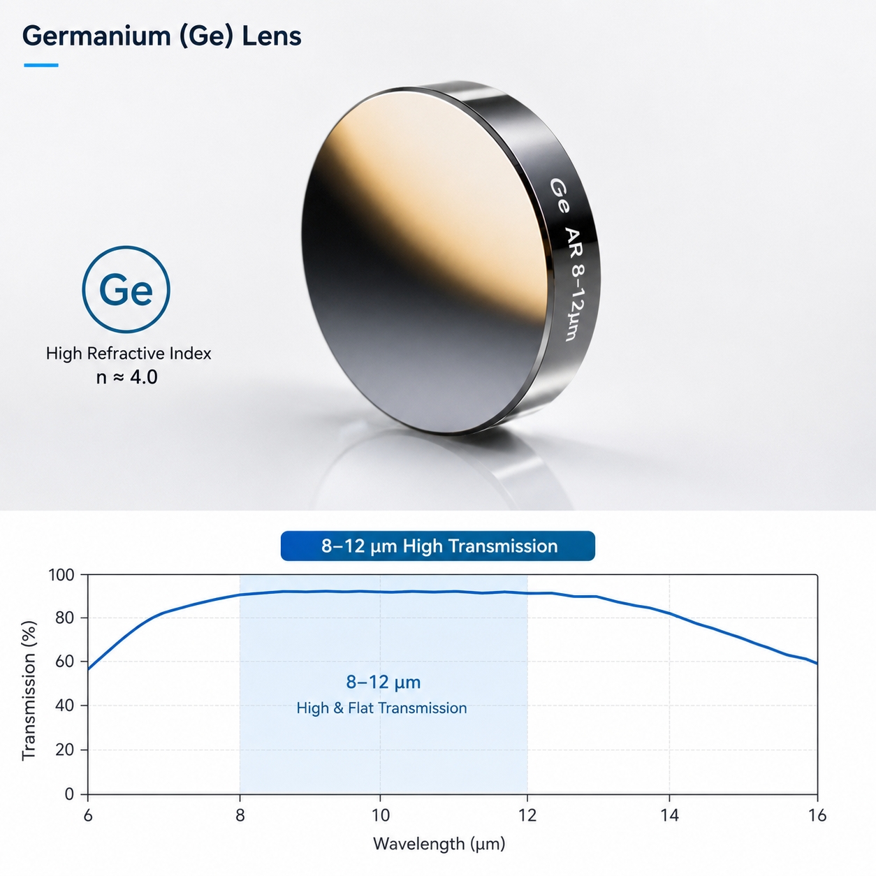
The metal housing not only provides mechanical protection but also participates in thermal management. For laser devices, this is especially important. The top optical window is the main entrance and exit for light. Its material and coating affect not only transmittance but also Fresnel reflection and compatibility with different operating wavelengths (such as 850 nm, 1310 nm, and 1550 nm).
The bottom pins are used for electrical signal input and output, and also determine the package size standards, such as the common TO-18, TO-56, and other specifications. These size standards directly affect the mounting method and spatial layout in subsequent system design.
TO Package and the 45° Reflecting Prism
In a standard TO package, the chip typically outputs light directly through the window along a preset optical axis. Optical path control occurs outside the package, using external lenses or coupling systems, so no internal light path redirection structure is needed.
However, in some special scenarios – for example, when a horizontally mounted laser diode chip needs to redirect its light to a vertical output direction – the standard solution cannot meet the requirement. In such cases, a 45° prism is introduced inside the TO package. The chip remains horizontally mounted for better heat dissipation and high-frequency performance, while the 45° prism precisely reflects the laterally emitted horizontal light into the vertical direction, exiting through the top cap. This achieves optical path redirection while maintaining package stability. Therefore, the standard TO package meets conventional direct-output requirements, while the 45° prism TO package provides an internally integrated solution for specific optical path layouts without sacrificing chip operating conditions.

Why the TO Package Exists in a Broader Packaging System
If you look at the TO package in isolation, it is easy to see it as just a simple housing. But in actual optoelectronic engineering, it is only the foundational level of a larger packaging system. As system complexity increases, different package forms have evolved to meet different integration needs.
For example, above the TO package is the BOX package. Its characteristic is that it integrates the light source and some optical components within a closed structure, allowing the optical path to be organized and folded to some extent internally. This makes it more suitable for systems with spatial layout requirements, such as gas detection or spectral analysis. In the communications field, a step above that is the butterfly package, which emphasizes long-term stability and precise control. It typically integrates TEC temperature control, multi-electrode control, and a monitoring photodiode to ensure wavelength stability of the laser output.
Why is it Still Widely Used Today?
From a technical perspective, the TO package is not the most advanced package form, but in many applications, it remains a very practical choice.
On one hand, its structure is highly standardized, facilitating mass production and system integration. On the other hand, its hermetic sealing ensures long-term stability. In low-to-medium power optical applications, such as common TO-can laser diodes or photodetectors, this structure already meets performance requirements.
Therefore, in terms of cost, reliability, and performance, the TO package provides a balanced solution. This is the main reason it has existed for so long.
Common Applications
In real systems, TO packages typically appear at key positions for optoelectronic conversion. For example, in TO-can laser diodes, they serve as the basic package providing a stable light output interface. In photodetectors, they are used to ensure alignment between the incident light and the detection area. In some optical communication modules (such as TOSA/ROSA) or sensing systems, TO packages also exist as standardized components because they are easy to install, replace, and integrate into systems. The common feature across these applications is a stable and repeatable optoelectronic interface.
What Are the Limitations of TO Packages?
Although TO packages perform stably in many scenarios, they do not provide complete optical functionality. They cannot actively control the beam shape, nor can they optimize beam uniformity or directionality. If the system has higher requirements for beam quality – such as needing collimation, shaping, or coupling into an optical fiber – additional optical design must be introduced.
At the same time, due to package structure limitations, alignment accuracy and thermal stability have certain boundaries. In high-precision systems, these factors often need to be compensated for through additional design. Therefore, the TO package is not a complete solution on its own.
The Role of Optical Components in TO Packages
Performance optimization of TO packages typically relies on optical components. For example, adding a collimating lens can reduce the divergence angle and improve the coupling efficiency. Using an aspherical lens can increase optical energy utilization within a limited space. In specific applications, optical filters can be used to control the operating band or suppress stray light. These optical components refine and complete the TO package through optimization.
Conclusion
The advantages of the TO package are its high degree of standardization, stable cost, and ability to quickly convert an optoelectronic chip into a usable device. This structure allows lasers and detectors to be mass-produced and integrated into different systems with a unified interface. This is why it has long occupied a fundamental position in industries such as optical communications and gas detection.
FAQ
Q1: What is the core function of a TO package in an optical system?
The core function of a TO package is not just to “protect the chip,” but to provide a standardized optoelectronic interface. It gives a laser diode or photodetector a stable mechanical reference, electrical connections, and a fixed light output position, allowing the device to be directly integrated into optical communication or optical detection systems.
Q2: What is the main difference between a TO package and a BOX package?
The TO package emphasizes a standard interface and is suitable for basic integration of a single light source or detector. The BOX package is more oriented toward system-level integration, allowing internal optical path organization, component combination, and even basic optical design. Therefore, TO is more fundamental, while BOX is more of a modular system.
Q3: Why do many gas detection systems still use TO packages?
Because gas detection systems typically require a stable, low-cost, and batch-consistent light source. The advantages of the TO package are its mature structure, stable performance, and ease of replacement – making it very suitable for applications where engineering stability is the priority.
Q4: What is the relationship between a TO package and optical design?
The TO package is not a structure independent of optical design – it is actually part of the optical system. It determines the initial light output conditions. Subsequent designs, such as lenses, prisms, or fiber coupling, are all optimized based on this foundation.
Q5: Can optical performance be improved through the TO package itself?
The TO package itself does not improve optical performance. Its role is to provide stability and standardization. Real performance improvement typically comes from chip design or subsequent optical system design, not from the package itself.